In the fast-paced world of technology, the demand for innovative solutions to memory limitations is at an all-time high. SanDisk, a leading DRAM/NAND maker, is stepping up to the challenge by proposing a groundbreaking solution: stacking NAND Flash within chips. This out-of-the-box approach is driven by the increasing need for compute power in the era of artificial intelligence (AI).
Addressing Memory Limitations with Innovative Solutions
The traditional reliance on DRAM as the primary memory component is facing challenges such as rising costs, development hurdles, and power consumption issues. Alternative technologies like High Bandwidth Memory (HBM) are struggling to keep up with demand, creating bottlenecks in the system.
HBM, with its limited capacities and proximity to the primary chip, poses latency drawbacks. On the other hand, NAND Flash offers higher capacities at a lower cost but suffers from slower data transfer speeds and inability to match the speed of DRAM.
The Fusion of DRAM & NAND Technologies
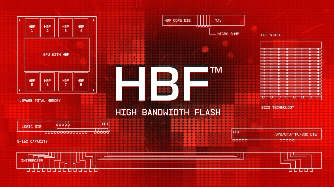
To bridge these gaps, SanDisk introduced its High-Bandwidth Flash (HBF) solution, which mirrors the architectural hierarchy of HBM by stacking multiple layers of NAND Flash. Each layer is interconnected using Through Silicon Vias (TSVs), creating a unified stack with capacities scaling up to 4 TB.
The latest breakthrough from SanDisk involves 3D stacking of a NAND Flash tile using CMOS Bonded Array (CBA) underneath the main compute tile, such as an AI accelerator or GPU. This approach leverages the strengths of both HBM DRAM for immediate memory needs and NAND Flash for read/write operations and larger data sets.
The integration of a multi-core processor directly onto a high-capacity, high-bandwidth non-volatile memory tile offers a glimpse into future technologies that can overcome memory bottlenecks. However, the transition from patent to reality requires addressing challenges like power efficiency, manufacturing costs, and more.
The strategic significance of SanDisk’s patent lies in its ability to create a unique architecture that combines the best of both DRAM and NAND technologies. While the road to standardization may be long, the promise of closing the gap between innovation and implementation is a story worth following closely.
In conclusion, SanDisk’s pioneering efforts in merging DRAM and NAND technologies within chips represent a significant step towards unlocking new possibilities in memory solutions. As the industry continues to evolve, the convergence of high-speed, high-capacity memory architectures will play a crucial role in shaping the future of computing.
Source: