Table of Contents
The Future of Intel’s 14A Process: A Game-Changer in the Tech World
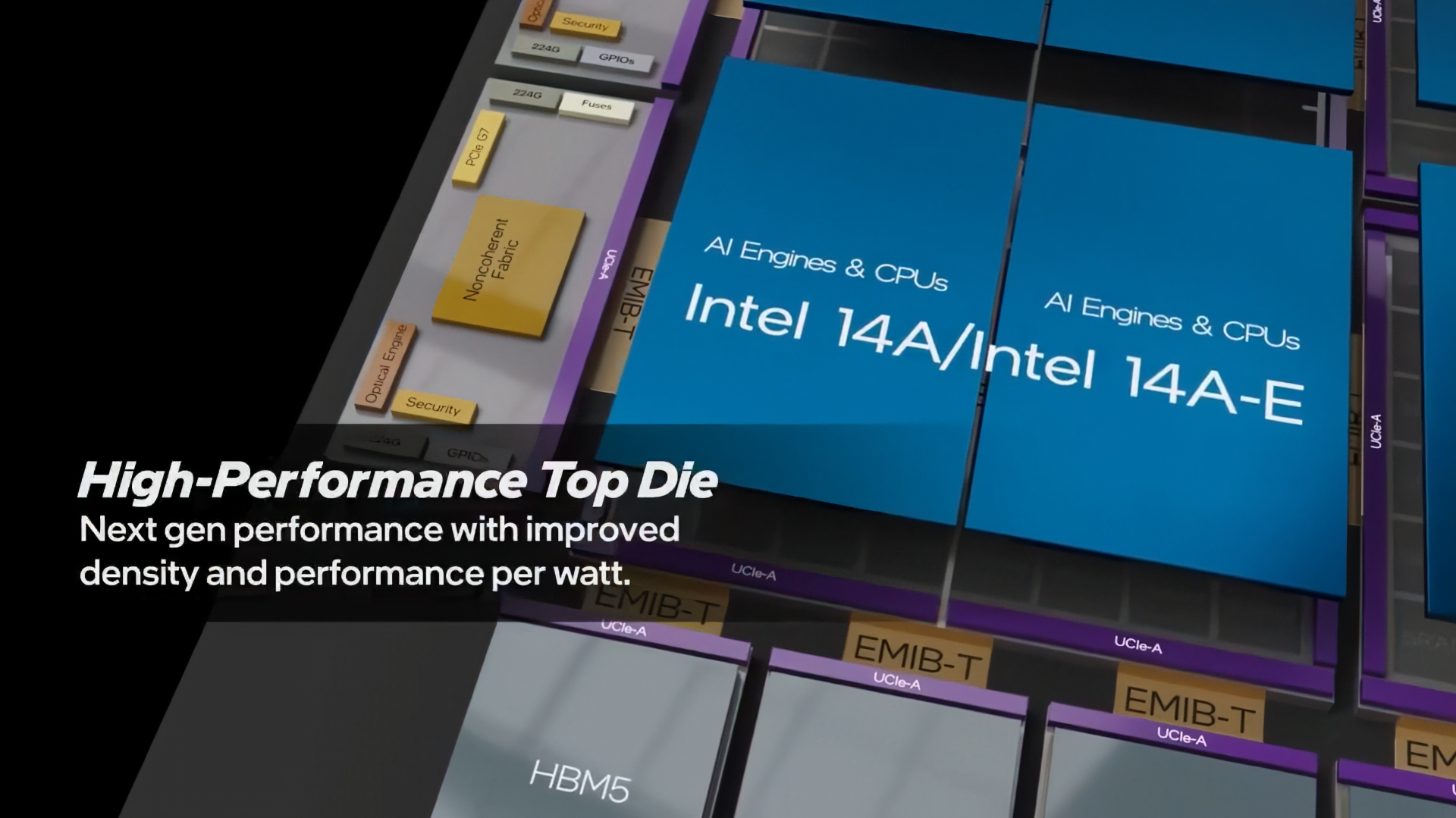
In the fast-paced world of technology, Intel’s next-gen 14A process is causing a stir. While there isn’t a confirmed anchor customer yet, the industry’s top players are closely evaluating this innovative solution. According to a recent investment note from Piper Sandler, the search for an alternative to TSMC has led to intense interest in Intel’s 14A process.
Piper Sandler’s Positive Outlook on Intel’s 14A Process
Piper Sandler’s analysis of Intel’s 14A process reveals a positive trend in technical data points. Major tech giants like Amazon, Apple, AMD, Google, Tesla, Microsoft, NVIDIA, and Qualcomm are actively assessing the potential of this next-gen technology amidst various industry dynamics.
Intel’s Impressive Technological Advances
Intel’s 14A node has shown significant progress, with a defect density of 0.5 achieved in June 2026. The company aims to further improve this to a D0 of 0.1 to 0.2 by Q1 2027. This indicates a promising trajectory towards commercialization as defect density decreases, leading to higher yields.
David Zinsner, from Intel, highlighted that the advancements in the 14A process are unprecedented since the 22nm era in 2012, showcasing Intel’s commitment to cutting-edge innovation.
The Quest for Alternatives to TSMC
With TSMC’s capacity constraints projected until 2028, the semiconductor industry is actively seeking alternatives. Intel emerges as a strong contender, especially with the political push for onshoring production. The 14A process presents a viable solution if it meets industry expectations.
Intel’s Strategic Capital-Raise Initiatives
Intel’s recent capital-raising efforts, totaling around $20 billion, signal the company’s confidence in securing anchor customers for the 14A process. Lip-Bu Tan’s cautious approach underscores the critical importance of confirmed deals before expanding Intel’s foundry capabilities.
The completion of Fab 62 and the upcoming investment in tooling costs reflect Intel’s readiness to scale production on the 14A node. This strategic planning aligns with Intel’s goal of commencing volume production by Q1 2028.
Key Features of Intel’s 14A Process
- A backside power delivery system named PowerDirect for enhanced efficiency.
- The RibbonFET 2 transistors and second-gen Gate-All-Around architecture for improved transistor performance.
Intel’s innovative technologies promise to revolutionize chip fabrication processes, setting new standards in the industry. With a strong focus on delivering cutting-edge solutions, Intel is poised to shape the future of semiconductor manufacturing.
In Conclusion
Intel’s 14A process represents a significant leap forward in semiconductor technology. With industry giants evaluating its potential and Intel’s strategic investments, the future looks promising for this innovative solution. As Intel continues to push boundaries and redefine industry standards, the 14A process stands out as a game-changer in the tech world.